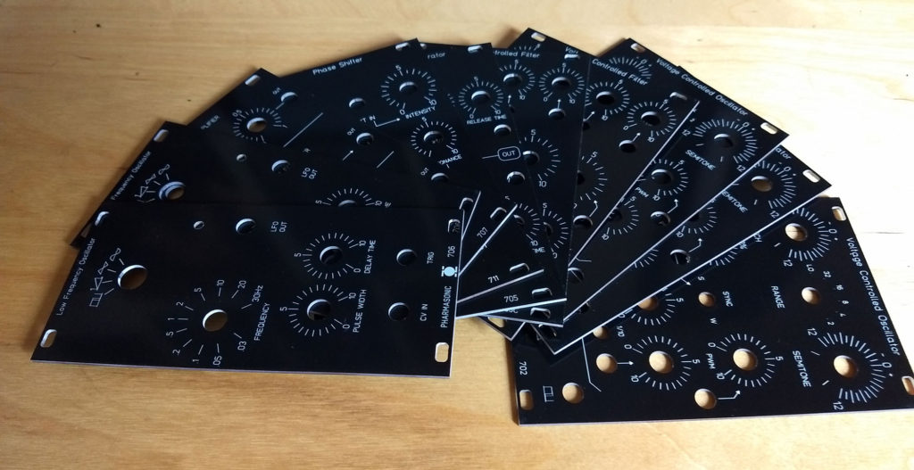
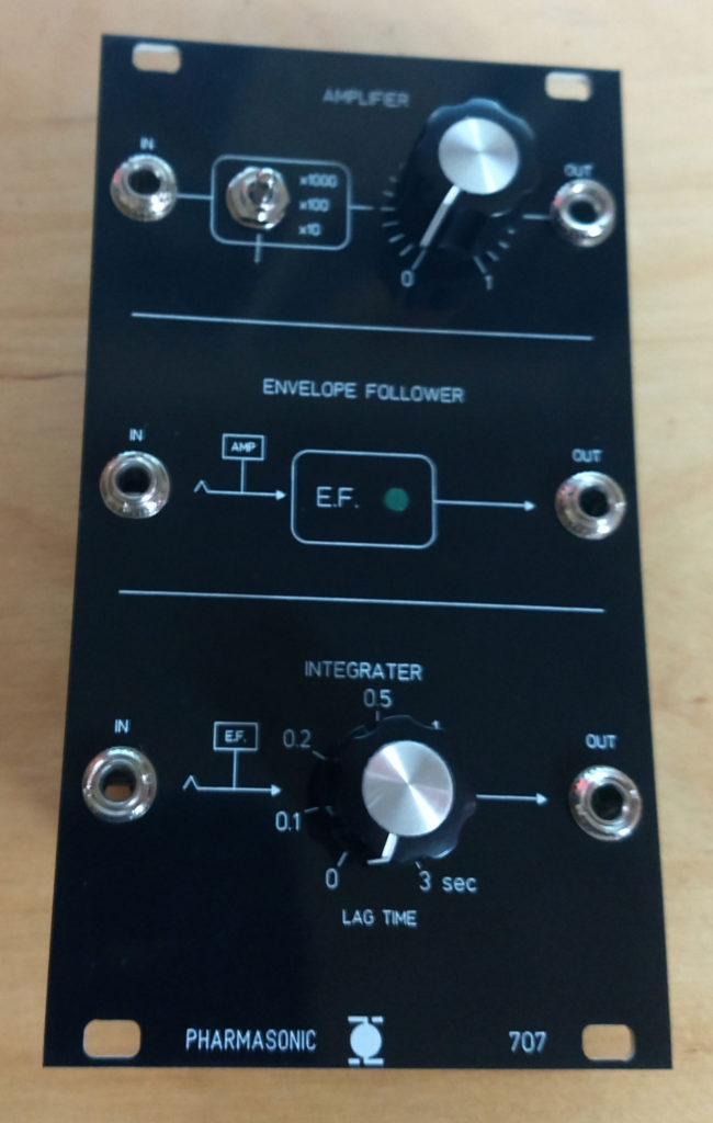
PCB’s arrived on Friday, while I was out of town for the weekend, of course. I was able to get home on Sunday in time to build out the patch bay and the noise source that day.
Monday was spent with the VCA’s. I built both at the same time, which did help cut down on time spent placing parts as I could look at the 1st one to put together the second by, and an assembly-line-esque setup of hitting each board with the soldering iron in sequence speeds up the time spent fiddling with things between soldering. Still, twice the boards means twice the number of bits to solder, so the process took probably 5-6 hours in total, which made for a long day after an 8 hour workday. I will probably need to pace myself on the more complex boards and/or multiple boards at once to stretch the build processes out across a couple sessions to keep myself from making mistakes due to overwork.
My process seems to be working well, which includes sorting all the resistors and caps into individual bins before starting to save me from hunting each down individually and mistaking one cap type for another. All the other bits come from a big bag of bits or from my case that holds all the transistors and IC’s for the project. It is organized enough to work without being overtly anal retentive.
Pictures!


